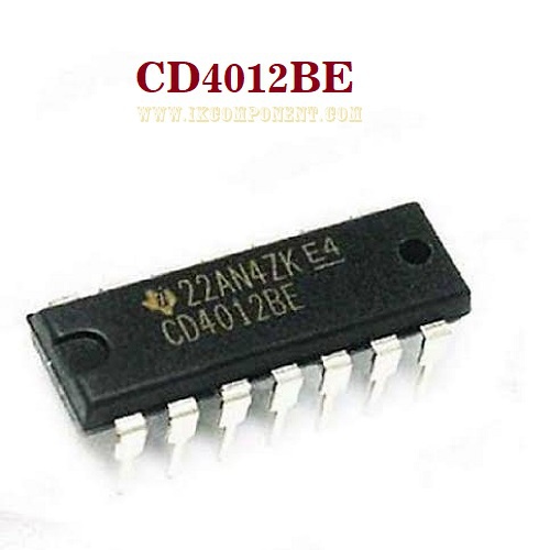
CD4012BE HEF4012BE HEF4012BE

Offer Zone Top Deals & Discounts
  • Home|
  • Product details
Price:

N200.00

Product description:
CD4012BE

Description

CD4011B, CD4012B, and CD4023B NAND gates provide the system designer with direct implementation of the NAND function and supplement the existing family of CMOS gates. All inputs and outputs are buffered.

The CD4011B, CD4012B, and CD4023B types are supplied in 14-lead hermetic dual-in-line ceramic packages (F3A suffix), 14-lead dual-in-line plastic packages (E suffix), 14-lead small-outline packages (M, MT, M96, and NSR suffixes), and 14-lead thin shrink small-outline packages (PWR suffix). The CD4011B and CD4023B types also are supplied in 14-lead thin shrink small-outline packages (PW suffix).

Features

  • Propagation delay time = 60 ns (typ.) at CL = 50 pF, VDD = 10 V
  • Buffered inputs and outputs
  • Standardized symmetrical output characteristics
  • Maximum input current of 1 µA at 18 V over-full package temperature range; 100 nA at 18 V and 25°C
  • 100% tested for quiescent current at 20 V
  • 5-V, 10-V, and 15-V parametric ratings
  • Noise margin (over full package temperature range:
        1 V at VDD = 5 V
        2 V at VDD = 10 V
        2.5 at VDD = 15 V
  • Meets all requirements of JEDEC Tentative Standard No. 13B, "Standard Specifications for Description of "B" Series CMOS Devices"

Quad 2 Input—CD4011B
Dual 4 Input—CD4012B
Triple 3 Input—CD4023B
Data sheet acquired from Harris Semiconductor.

Product category:
integrated Circuits
1645
Quantity:


© 2026 Ikcomponents Store. All rights reserved | Designed by Chrikinex.


